ChipFind - документация

Электронный компонент: MSP430F168IPM

Скачать:  PDF   ZIP

Document Outline

MSP430x15x, MSP430x16x, MSP430x161x
MIXED SIGNAL MICROCONTROLLER
SLAS368D- OCTOBER 2002- REVISED MARCH 2005
1
POST OFFICE BOX 655303
DALLAS, TEXAS 75265
D
Low Supply-Voltage Range, 1.8 V . . . 3.6 V
D
Ultralow-Power Consumption:
- Active Mode: 330
A at 1 MHz, 2.2 V
- Standby Mode: 1.1
A
- Off Mode (RAM Retention): 0.2
A
D
Five Power-Saving Modes
D
Wake-Up From Standby Mode in less
than 6
s
D
16-Bit RISC Architecture, 125-ns
Instruction Cycle Time
D
Three-Channel Internal DMA
D
12-Bit A/D Converter With Internal
Reference, Sample-and-Hold and Autoscan
Feature
D
Dual 12-Bit D/A Converters With
Synchronization
D
16-Bit Timer_A With Three
Capture/Compare Registers
D
16-Bit Timer_B With Three or Seven
Capture/Compare-With-Shadow Registers
D
On-Chip Comparator
D
Serial Communication Interface (USART0),
Functions as Asynchronous UART or
Synchronous SPI or I
2
C
TM
Interface
D
Serial Communication Interface (USART1),
Functions as Asynchronous UART or
Synchronous SPI Interface
D
Supply Voltage Supervisor/Monitor With
Programmable Level Detection
D
Brownout Detector
D
Bootstrap Loader
I
2
C is a registered trademark of Philips Incorporated.
D
Serial Onboard Programming,
No External Programming Voltage Needed
Programmable Code Protection by Security
Fuse
D
Family Members Include:
- MSP430F155:
16KB+256B Flash Memory
512B RAM
- MSP430F156:
24KB+256B Flash Memory
1KB RAM
- MSP430F157:
32KB+256B Flash Memory,
1KB RAM
- MSP430F167:
32KB+256B Flash Memory,
1KB RAM
- MSP430F168:
48KB+256B Flash Memory,
2KB RAM
- MSP430F169:
60KB+256B Flash Memory,
2KB RAM
- MSP430F1610:
32KB+256B Flash Memory
5KB RAM
- MSP430F1611:
48KB+256B Flash Memory
10KB RAM
- MSP430F1612:
55KB+256B Flash Memory
5KB RAM
D
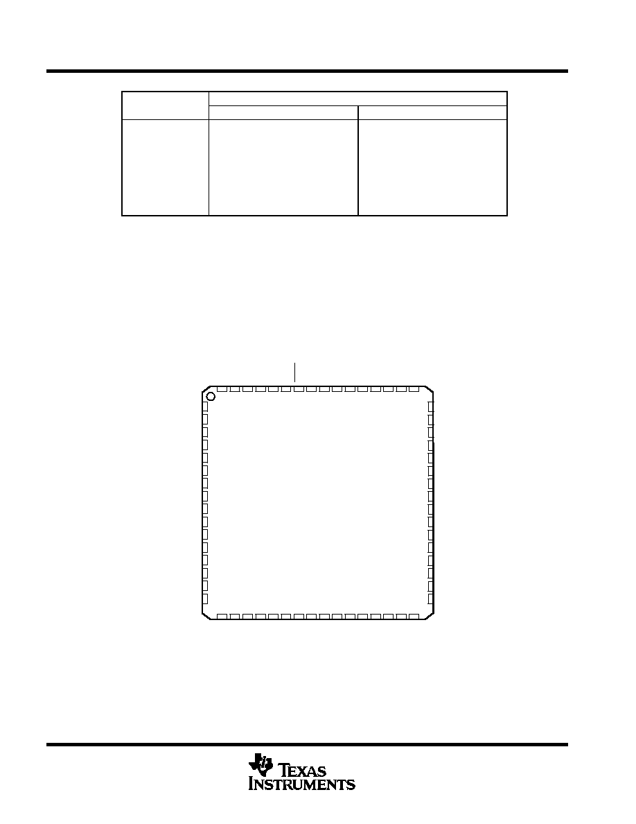
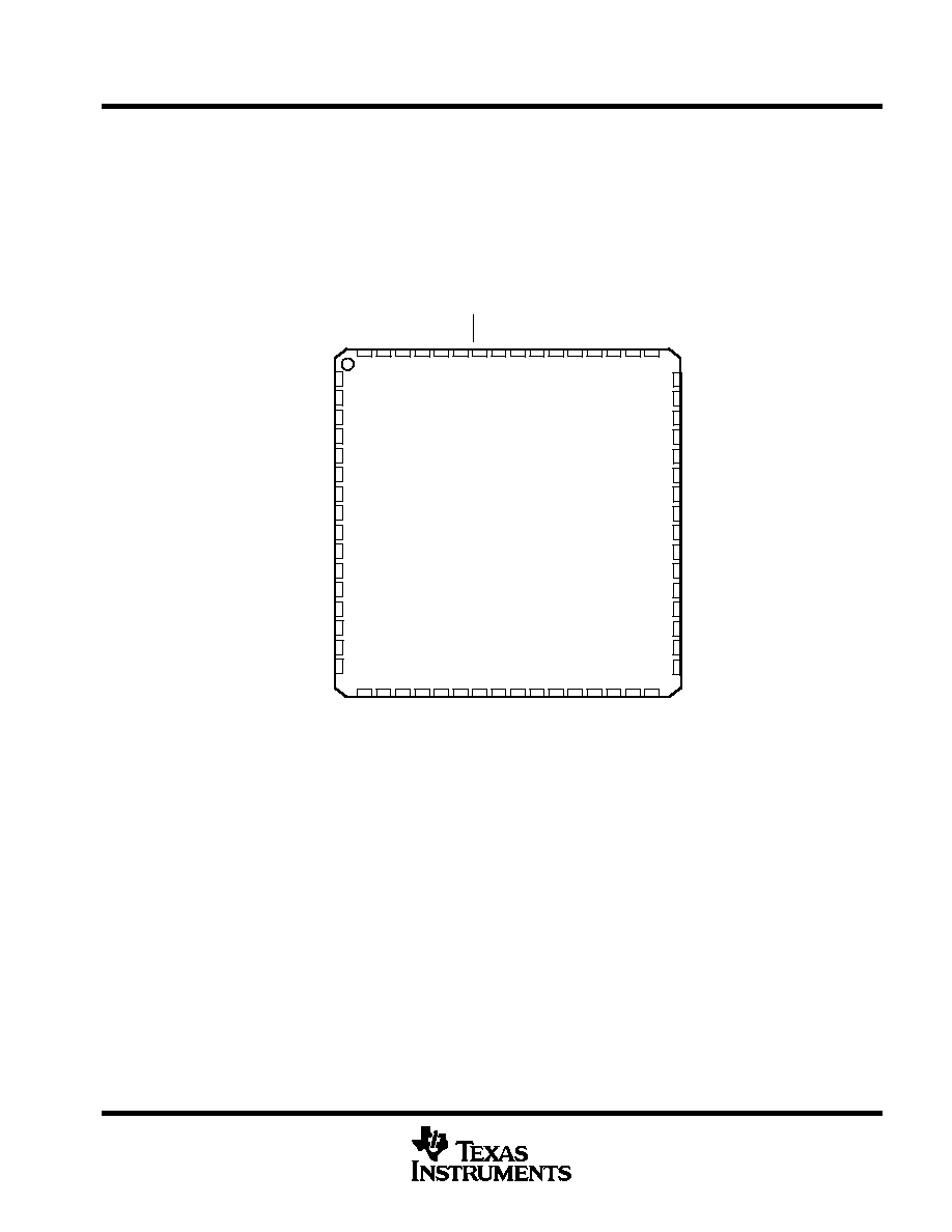
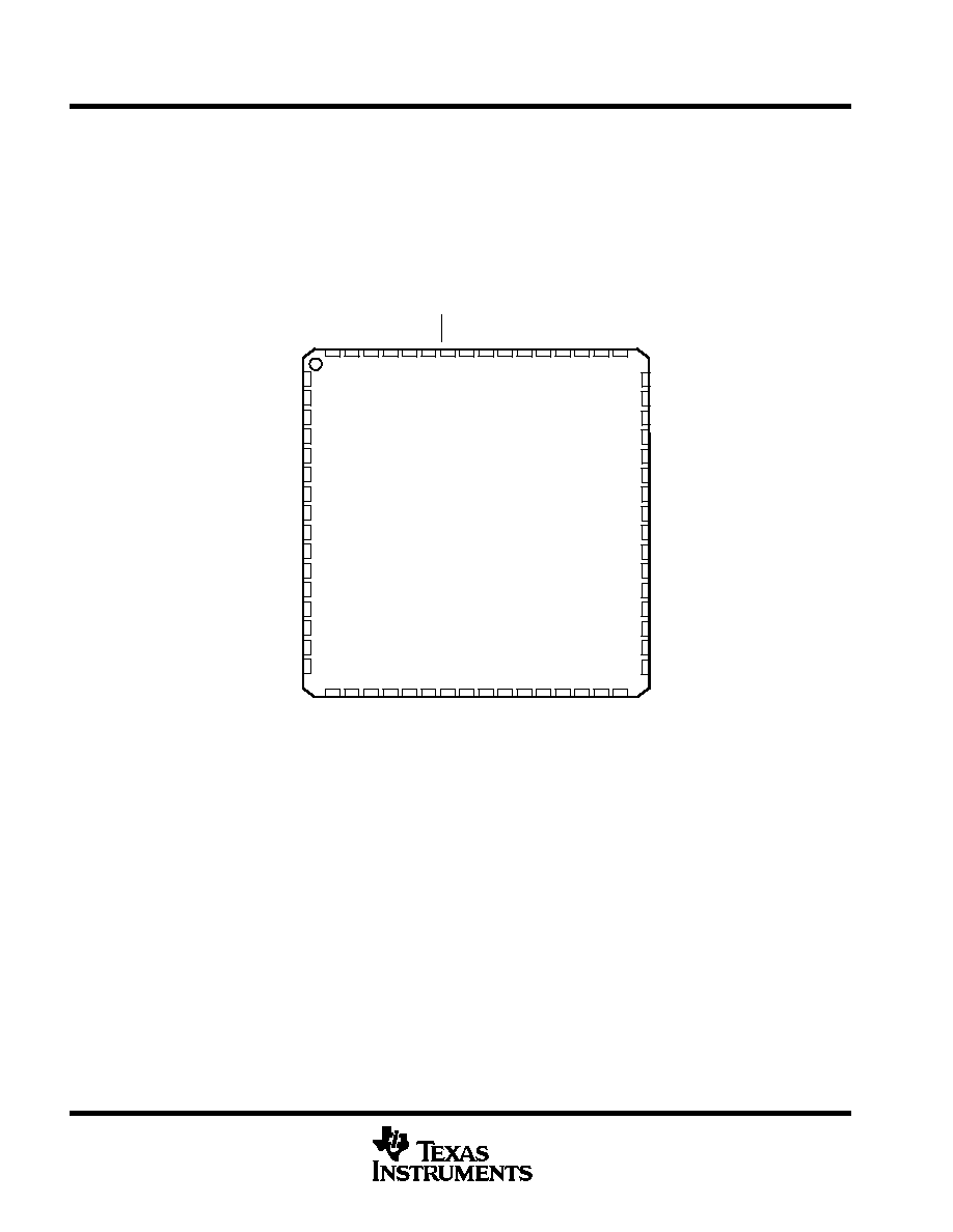
Available in 64-Pin Quad Flat Pack (QFP)
and 64-pin QFN (see Available Options)
D
For Complete Module Descriptions, See the
MSP430x1xx Family User's Guide,
Literature Number SLAU049
description
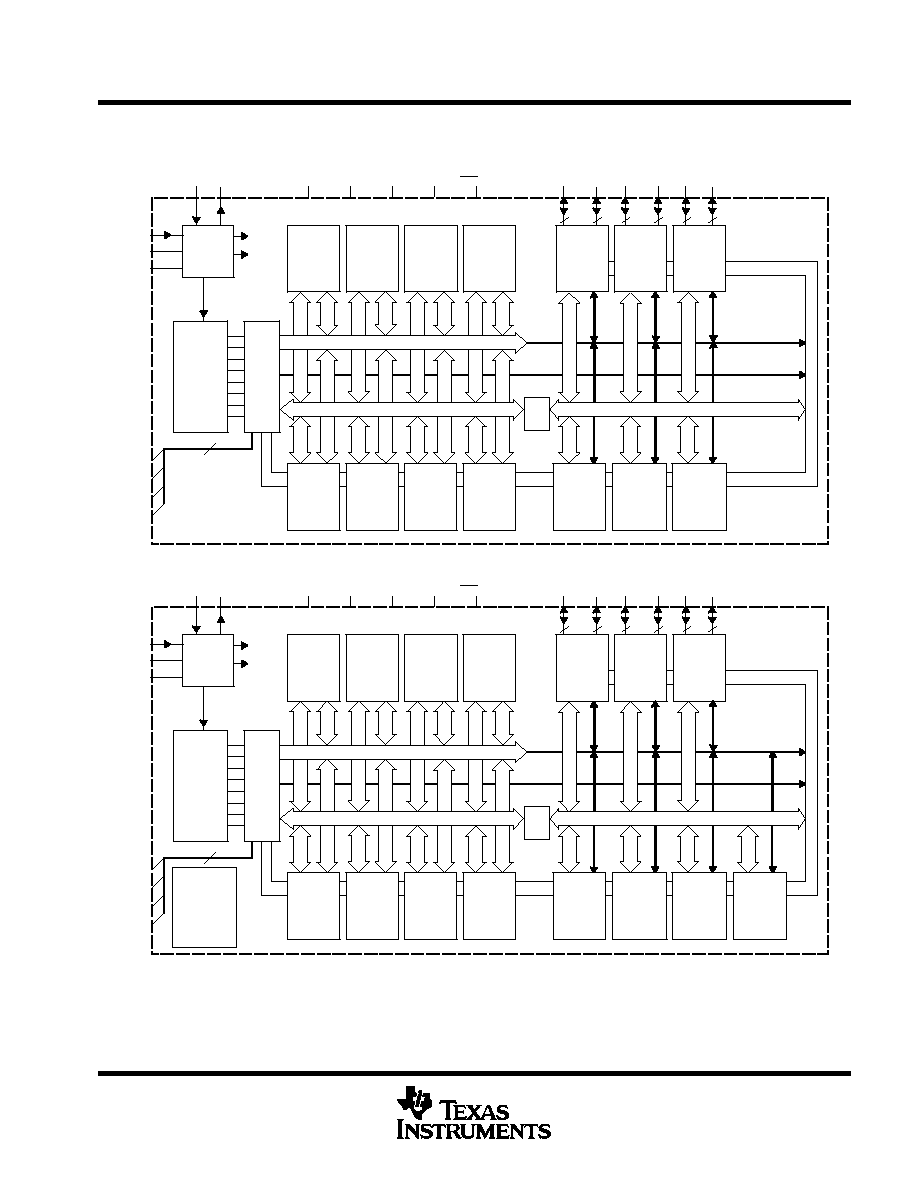
The Texas Instruments MSP430 family of ultralow power microcontrollers consist of several devices featuring
different sets of peripherals targeted for various applications. The architecture, combined with five low power
modes is optimized to achieve extended battery life in portable measurement applications. The device features
a powerful 16-bit RISC CPU, 16-bit registers, and constant generators that attribute to maximum code efficiency.
The digitally controlled oscillator (DCO) allows wake-up from low-power modes to active mode in less than 6
s.
The MSP430x15x/16x/161x series are microcontroller configurations with two built-in 16-bit timers, a fast 12-bit
A/D converter, dual 12-bit D/A converter, one or two universal serial synchronous/asynchronous
communication interfaces (USART), I
2
C, DMA, and 48 I/O pins. In addition, the MSP430x161x series offers
extended RAM addressing for memory-intensive applications and large C-stack requirements.
Typical applications include sensor systems, industrial control applications, hand-held meters, etc.
Copyright
2002 - 2005, Texas Instruments Incorporated
PRODUCTION DATA information is current as of publication date.
Products conform to specifications per the terms of Texas Instruments
standard warranty. Production processing does not necessarily include
testing of all parameters.
Please be aware that an important notice concerning availability, standard warranty, and use in critical applications of
Texas Instruments semiconductor products and disclaimers thereto appears at the end of this data sheet.
MSP430x15x, MSP430x16x, MSP430x161x
MIXED SIGNAL MICROCONTROLLER
SLAS368D- OCTOBER 2002- REVISED MARCH 2005
2
POST OFFICE BOX 655303
DALLAS, TEXAS 75265
AVAILABLE OPTIONS
PACKAGED DEVICES
T
A
PLASTIC 64-PIN QFP (PM)
PLASTIC 64-PIN QFN (RTD)
-40
C to 85
C
MSP430F155IPM
MSP430F156IPM
MSP430F157IPM
MSP430F167IPM
MSP430F168IPM
MSP430F169IPM
MSP430F1610IPM
MSP430F1611IPM
MSP430F1612IPM
MSP430F155IRTD
MSP430F156IRTD
MSP430F157IRTD
MSP430F167IRTD
MSP430F168IRTD
MSP430F169IRTD
MSP430F1610IRTD
MSP430F1611IRTD
MSP430F1612IRTD
Product Preview
pin designation, MSP430F155, MSP430F156, and MSP430F157
17 18 19
P5.4/MCLK
P5.3
P5.2
P5.1
P5.0
P4.7/TBCLK
P4.6
P4.5
P4.4
P4.3
P4.2/TB2
P4.1/TB1
P4.0/TB0
P3.7
P3.6
P3.5/URXD0
48
47
46
45
44
43
42
41
40
39
38
37
36
35
34
33
20
1
2
3
4
5
6
7
8
9
10
11
12
13
14
15
16
DV
CC
P6.3/A3
P6.4/A4
P6.5/A5
P6.6/A6/DAC0
P6.7/A7/DAC1/SVSIN
V
REF+
XIN
XOUT
Ve
REF+
V
REF-
/Ve
REF-
P1.0/TACLK
P1.1/TA0
P1.2/TA1
P1.3/TA2
P1.4/SMCLK
21 22 23 24
63 62 61 60 59
64
58
56 55 54
57
25 26 27 28 29
53 52 51 50 49
30 31 32
PM, RTD PACKAGE
(TOP VIEW)
AV
CC
DV
SS
AV
SS
P6.2/A2
P6.1/A1
P6.0/A0
RST
/NMI
TCK
TMS
TDI/TCLK
TDO/TDI
XT2IN
XT2OUT
P5.7/TBOUTH/SVSOUT
P5.6/ACLK
P5.5/SMCLK
P1.5/T
A0
P1.6/T
A1
P1.7/T
A2
P2.0/ACLK
P2.1/T
AINCLK
P2.2/CAOUT/T
A0
P2.3/CA0/T
A1
P2.4/CA1/T
A2
P2.5/R
OSC
P2.6/ADC12CLK/DMAE0
P2.7/T
A0
P3.0/STE0
P3.1/SIMO0/SDA
P3.2/SOMI0
P3.3/UCLK0/SCL
P3.4/UTXD0
MSP430x15x, MSP430x16x, MSP430x161x
MIXED SIGNAL MICROCONTROLLER
SLAS368D- OCTOBER 2002- REVISED MARCH 2005
3
POST OFFICE BOX 655303
DALLAS, TEXAS 75265
pin designation, MSP430F167, MSP430F168, MSP430F169
17 18 19
P5.4/MCLK
P5.3/UCLK1
P5.2/SOMI1
P5.1/SIMO1
P5.0/STE1
P4.7/TBCLK
P4.6/TB6
P4.5/TB5
P4.4/TB4
P4.3/TB3
P4.2/TB2
P4.1/TB1
P4.0/TB0
P3.7/URXD1
P3.6/UTXD1
P3.5/URXD0
48
47
46
45
44
43
42
41
40
39
38
37
36
35
34
33
20
1
2
3
4
5
6
7
8
9
10
11
12
13
14
15
16
DV
CC
P6.3/A3
P6.4/A4
P6.5/A5
P6.6/A6/DAC0
P6.7/A7/DAC1/SVSIN
V
REF+
XIN
XOUT
Ve
REF+
V
REF-
/Ve
REF-
P1.0/TACLK
P1.1/TA0
P1.2/TA1
P1.3/TA2
P1.4/SMCLK
21 22 23 24
63 62 61 60 59
64
58
56 55 54
57
25 26 27 28 29
53 52 51 50 49
30 31 32
PM, RTD PACKAGE
(TOP VIEW)
AV
CC
DV
SS
AV
SS
P6.2/A2
P6.1/A1
P6.0/A0
RST
/NMI
TCK
TMS
TDI/TCLK
TDO/TDI
XT2IN
XT2OUT
P5.7/TBOUTH/SVSOUT
P5.6/ACLK
P5.5/SMCLK
P1.5/T
A0
P1.6/T
A1
P1.7/T
A2
P2.0/ACLK
P2.1/T
AINCLK
P2.2/CAOUT/T
A0
P2.3/CA0/T
A1
P2.4/CA1/T
A2
P2.5/R
OSC
P2.6/ADC12CLK/DMAE0
P2.7/T
A0
P3.0/STE0
P3.1/SIMO0/SDA
P3.2/SOMI0
P3.3/UCLK0/SCL
P3.4/UTXD0
MSP430x15x, MSP430x16x, MSP430x161x
MIXED SIGNAL MICROCONTROLLER
SLAS368D- OCTOBER 2002- REVISED MARCH 2005
4
POST OFFICE BOX 655303
DALLAS, TEXAS 75265
pin designation, MSP430F1610, MSP430F1611, MSP430F1612
17 18 19
P5.4/MCLK
P5.3/UCLK1
P5.2/SOMI1
P5.1/SIMO1
P5.0/STE1
P4.7/TBCLK
P4.6/TB6
P4.5/TB5
P4.4/TB4
P4.3/TB3
P4.2/TB2
P4.1/TB1
P4.0/TB0
P3.7/URXD1
P3.6/UTXD1
P3.5/URXD0
48
47
46
45
44
43
42
41
40
39
38
37
36
35
34
33
20
1
2
3
4
5
6
7
8
9
10
11
12
13
14
15
16
DV
CC
P6.3/A3
P6.4/A4
P6.5/A5
P6.6/A6/DAC0
P6.7/A7/DAC1/SVSIN
V
REF+
XIN
XOUT
Ve
REF+
V
REF-
/Ve
REF-
P1.0/TACLK
P1.1/TA0
P1.2/TA1
P1.3/TA2
P1.4/SMCLK
21 22 23 24
63 62 61 60 59
64
58
56 55 54
57
25 26 27 28 29
53 52 51 50 49
30 31 32
PM, RTD PACKAGE
(TOP VIEW)
AV
CC
DV
SS
AV
SS
P6.2/A2
P6.1/A1
P6.0/A0
RST
/NMI
TCK
TMS
TDI/TCLK
TDO/TDI
XT2IN
XT2OUT
P5.7/TBOUTH/SVSOUT
P5.6/ACLK
P5.5/SMCLK
P1.5/T
A0
P1.6/T
A1
P1.7/T
A2
P2.0/ACLK
P2.1/T
AINCLK
P2.2/CAOUT/T
A0
P2.3/CA0/T
A1
P2.4/CA1/T
A2
P2.5/R
OSC
P2.6/ADC12CLK/DMAE0
P2.7/T
A0
P3.0/STE0
P3.1/SIMO0/SDA
P3.2/SOMI0
P3.3/UCLK0/SCL
P3.4/UTXD0
MSP430x15x, MSP430x16x, MSP430x161x
MIXED SIGNAL MICROCONTROLLER
SLAS368D- OCTOBER 2002- REVISED MARCH 2005
5
POST OFFICE BOX 655303
DALLAS, TEXAS 75265
functional block diagrams
MSP430x15x
Oscillator
ACLK
SMCLK
CPU
Incl. 16 Reg.
Bus
Conv
MCB
XIN
XOUT
P3
P4
P2
XT2IN
XT2OUT
TMS
TCK
MDB, 16 Bit
MAB, 16 Bit
MCLK
4
TDI/TCLK
TDO/TDI
P5
P6
MAB,
4 Bit
DV
CC
DV
SS
AV
CC
AV
SS
RST/NMI
System
Clock
R
OSC
P1
32KB Flash
24KB Flash
16KB Flash
1KB RAM
1KB RAM
512B RAM
ADC12
12-Bit
8 Channels
<10
s Conv.
DAC12
12-Bit
2 Channels
Voltage out
DMA
Controller
3 Channels
Watchdog
Timer
15/16-Bit
Timer_B3
3 CC Reg
Shadow
Reg
Timer_A3
3 CC Reg
Test
JTAG
Emulation
Module
I/O Port 1/2
16 I/Os,
with
Interrupt
Capability
I/O Port 3/4
16 I/Os
POR
SVS
Brownout
Comparator
A
USART0
UART Mode
SPI Mode
I
2
C Mode
I/O Port 5/6
16 I/Os
MDB, 8 Bit
MDB, 16-Bit
MAB, 16-Bit
8
8
8
8
8
8
MSP430x16x
Oscillator
ACLK
SMCLK
CPU
Incl. 16 Reg.
Bus
Conv
MCB
XIN
XOUT
P3
P4
P2
XT2IN
XT2OUT
TMS
TCK
MDB, 16 Bit
MAB, 16 Bit
MCLK
4
TDI/TCLK
TDO/TDI
P5
P6
MAB,
4 Bit
DV
CC
DV
SS
AV
CC
AV
SS
RST/NMI
System
Clock
R
OSC
P1
Hardware
Multiplier
MPY, MPYS
MAC,MACS
60KB Flash
48KB Flash
32KB Flash
2KB RAM
2KB RAM
1KB RAM
ADC12
12-Bit
8 Channels
<10
s Conv.
DAC12
12-Bit
2 Channels
Voltage out
DMA
Controller
3 Channels
Watchdog
Timer
15/16-Bit
Timer_B7
7 CC Reg
Shadow
Reg
Timer_A3
3 CC Reg
Test
JTAG
Emulation
Module
I/O Port 1/2
16 I/Os,
with
Interrupt
Capability
I/O Port 3/4
16 I/Os
POR
SVS
Brownout
Comparator
A
USART0
UART Mode
SPI Mode
I
2
C Mode
USART1
UART Mode
SPI Mode
I/O Port 5/6
16 I/Os
MDB, 8 Bit
MDB, 16-Bit
MAB, 16-Bit
8
8
8
8
8
8